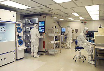
 | Scientists working in the new Clean Room don special gear to reduce the chance that dust and other particles will interfere with the creation of the mini- and nano-devices being built there. |
On Oct. 31, Yale dedicated the new Center for Microelectronics Materials
and Structures Clean Room, an $8 million, 2,600-square-foot facility for fabricating
micro- and nano-scale devices for engineering research.
T H I S
Yale dedicates $8 million Clean Room
“The number of Yale faculty members who are using micro- and nano-devices
in their research has grown dramatically in recent years,” said Paul Fleury,
dean of the Yale Engineering, “and so has the need for a facility where
these devices, with their ever-finer spatial detail and complexity, can be fabricated.”
The new Clean Room expands and updates the Center for Microelectronics Materials
and Structures, originally designed and built nearly 20 years ago with generous
gifts from the Keck Foundation, Jones Bequest, alumnus Vincent Coates and his
company Nanometrics, the IBM Corporation and others. Located on the fifth floor
of the Becton Engineering and Applied Science Center on Prospect Street, the
center serves over a dozen research groups, nearly 40 students in engineering
and an increasing number of collaborators.
“The original facility was a tremendous boost to our research capability
in the 1980s,” said Professor T.P. Ma, co-director of the center, “and
the new Clean Room reflects the considerable advances in technology since then.
It ensures Yale will remain on the cutting edge of this research.”
According to Professor Robert Schoelkopf, co-director of the center, the
new Clean Room facility will enable many kinds of novel research and will benefit
other University programs, especially those associated with the Yale Institute
for Nanoscience and Quantum Engineering, and the Yale National Science Foundation
Materials Research Science and Engineering Center.
With direct funding from the Provost’s Office, construction began in early
2007 after a year of planning. Two professional technical staff members have
also been added to provide support for users of the facility.
The Clean Room incorporates new environmental systems, utilities and digital
controls, and has state-of-the-art safety equipment and fireproofing. It features
lines for de-ionized and processed chilled water, a house vacuum and inert gas,
as well as upgrades for improved ventilation and toxic gas monitoring. The facility
will house equipment for optical lithography and photomask production, as well
as dry- and plasma-etching. It includes nearly 1,000 square feet of class-100
space (ultra-clean space that contains no more than 100 microscopic particles
per cubic foot of air), which includes lithography and wet processing bays.
“This major investment is one of many in our ongoing program for development
of science and engineering at Yale,” said Bruce Carmichael, associate provost
for science and technology. W E E K ' S
 S T O R I E S
![]()
 Todai-Yale venture to boost Japanese Studies in the U.S.
![]()
![]()
 Yale dedicates $8 million Clean Room
![]()
![]()
 For some infants, mother’s milk can help increase IQ, says study
![]()
![]()
 Engineering lessons get real-world application . . .
![]()
![]()
 ENDOWED PROFESSORSHIPS
 Mark Ashton appointed the Jesup Professor of Silviculture
![]()
 Alicia Schmidt Camacho named Sarai Ribicoff Associate Professor
![]()
![]()
 School of Public Health launches new Advanced Professional . . .
![]()
![]()
 Shareholder activist creates fund at Yale center for corporate governance
![]()
![]()
 Yale ceremony to commemorate Veteran’s Day
![]()
![]()
 Procrastination is not an option at Dissertation Boot Camp
![]()
![]()
 Show features Chinese artist’s works of ‘Revolution and Rebirth’
![]()
![]()
 IN MEMORIAM
 George Hersey: Wrote widely on art history and architecture
![]()
 Eugene Waith: Expert on Elizabethan and Jacobean theater
![]()
![]()
 From the United Way: ‘A Tale of Guiding Young Fathers’
![]()
![]()
 Program to look at company developing innovative . . .
![]()
![]()
 Campus Notes
![]()
Bulletin Home |
| Visiting on Campus
 |
| Calendar of Events
 |
| In the News
![]()
Bulletin Board |
| Classified Ads
 |
| Search Archives
 |
| Deadlines
![]()
Bulletin Staff |
| Public Affairs
 |
| News Releases
 |
| E-Mail Us
 |
| Yale Home